Authors
Publication
Pub Details
Date
Pages
ROM/RAM Immaterial
As a result of my article “Your Timex-Sinclair Can Become a Remote Terminal” (Sync 2:6) a number of readers raised questions concerning the peculiarities resulting from attempting to use memory-mapped I/O devices mapped to addresses not affected by the use of a RAM pack. I have seen many references to the strange effects of PEEKing and POKEing at addresses outside of the 16K to 32K range on a Sinclair, so I decided to spend a rainy afternoon investigating the various phenomena, and, more to the point, how to wire around these effects.
Various Standards
The address lines on the Z80A CPU are numbered from A0 to A15. These lines can be compared to the equivalent bits in a two-byte address: A0=1 when “on”, A1=2, … A10=1024, A11=2048, A12=4096, A13=8192, A14=16384 and A15=32768. Thus, when all address lines are high, you have a maximum value of 64K (or 65535), and, when all are low, you have an address of 0.
Note that above I referred to all address lines being “high”. With normal TTL (transistor to transistor logic), an active line is normally low voltage (or grounded), and an inactive line is high (or 4-5 volts). The reverse is true for the data and address lines on the Z80A CPU for some reason known only to the designers, so a “1” is high or +5 volts, and a “0” is indicated by a grounded or low voltage line.
Since the 1K ZX81 is the only machine on which I have had actual hands-on experience, the remarks on the ZX80 and the TS1000 are assumptions based only on what I have read about those computers, and from examination of their circuit diagrams. Where they differ drastically from the ZX81 I will mention them specifically.
The Strange Effects
As an initial demonstration, detach any add-ons from the CPU so that you have a plain unadorned 1K or 2K machine. Now enter the following little program:
1 REM ABCIf you now PRINT PEEK 16514, you will get a 38 printed on the screen. This is the value of the A in the REM. If you then PRINT PEEK 49282 (32K off the start of the REM and well off the end of the on-board RAM), you will find the same value printed. If you then POKE 49282,39 and LIST your little program, you will discover that the first statement is now 1 REM BBC. What you have done is to POKE a value way off the end of your memory but which changed your actual RAM contents anyway.
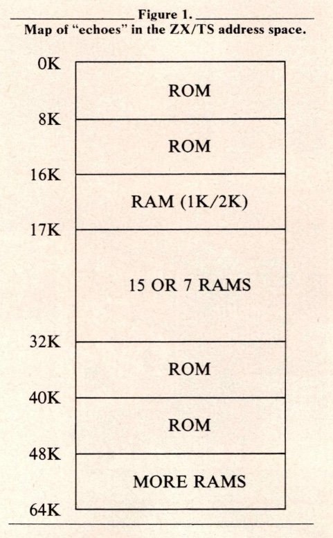
Another interesting demonstration is to PRINT PEEK 0, PEEK 32768 and the two answers will be the same. PRINT PEEK 0, PEEK 8192 has the same effect. To make things even more confusing, you will find echoes of the REM statement above every 1K throughout the addressing space (2K probably for a TS1000), except in those spots where the ‘ghost’ ROMs are hiding. The resulting map of the various echoes is illustrated in Figure 1.
The Causes
Apparently the designers of the original Sinclair decided that a maximum 16K RAM would be added, so the entire address space above 32K was ignored for the sake of a simplified internal layout. Additionally, since the RAM started at 16K and the ROM was only 4K or 8K long, the space between the end of ROM and the start of RAM was ignored as well.
Electronically speaking, line A15 is connected only to the keyboard and nothing else inside the Sinclair. This results in addresses above 32K being identified by the on-board chips as the address less the value of A15 (i.e., the address less 32K). Thus the duplicated RAM addresses. When the ROM is accessed (when A14 is low producing a resulting address less than 16K), A13 is ignored so that an address over 8K is interpreted as the address minus the value of A13 (or 8192).
Eliminating the Effects
Since all these ROMs and RAMs are running around the address space, how do you get rid of them so you can do some useful work? Luckily for us, the designers of the Sinclair gave us a couple of very potent levers to work with (except on the ZX80 they forgot one).
RAMCS (pin 2 on the top of the back edge connector) enables or disables the on-board 1K or 2K RAM. If this line is pulled low, either by the Sinclair or by some of your wiring, the on-board RAM is enabled and will answer. The 16K RAM pack connects this line directly to +5 volts, permanently disabling the onboard RAM. This is why adding a 16K RAM pack gives you 16K of RAM, not 17.
ROMCS (pin 23 on the lower edge connector) will engage or disengage the ROM chip. This pin should be very cautiously approached because tying it high at an inappropriate nanosecond will result in the Sinclair’s brain disappearing suddenly.
This is the line they unfortunately forgot to bring to the outside world on the ZX80. You can provide your own (if you have sufficient courage and faith) by soldering a jumper from the edge connector lower contact 23 (if there is one) to the ROM pin 20. This pin (ROM 20) should be connected originally to IC6 (a 74LS157) pin 7. Carefully cut this trace and bridge the gap with a 1.8K resistor. I give no guarantees on this, having never tried it, but I have seen it suggested in several places by people who should know what they are doing.
Addressing Schemes—The 74LS138
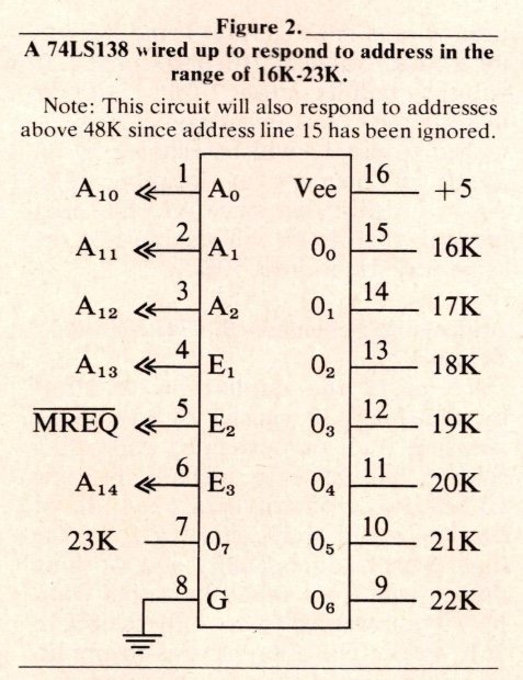
Enough of explanations, and on to some specific details for adding new chips. The building block of the addressing schemes which I use is the versatile 74LS138, Figure 2 shows a 74LS138 wired up to select chips at addresses 16K to 23K in steps of 1K. The chip select lines coming out of this chip are controlled as follows:
Pins 4, 5, and 6 are three enable chip lines. For the 74LS138 to be enabled, pins 4 and 5 must be low, and pin 6 high, all at the same moment. Although this may sound strange and complicated superficially, it is actually very useful because it eliminates the need for external decoding chips (in simple circuits). Remembering the ‘values’ of the various address lines, we can see that if A13 is low and A14 is high, the resulting address must be between 16K and 23K. (In keeping with on-board Sinclair technology A15 is ignored in this diagram).
Pins 1, 2, and 3 are designated as AO, A1, and A2 on the LS138. This designation pertains only to the pins on the LS138 and is in no way to be confused with the address lines on the Z80A of the same names. When the LS138 is enabled by the correct values applied to the enable pins, the values of the lines connected to the address input pins 1, 2, and 3 are added together. (In binary again: A0=1, A1=2, A2=4 when high, so a maximum of 7 is possible, with a minimum of 0, hence the 8 output labelled 00 to 07). The output pin with the designation of the binary total of the address inputs is then pulled LOW until the LS138 is disabled again.
Referring again to Figure 2, if A13 is low (8192=0), A14 is high (16384=1) and MREQ is low (memory access requested). The LS 138 is enabled.
If CPU line A11 is high (2048=1), and lines A10 (1024) and A12 (4096) are low (=0), then the LS138 sees its address inputs A0=0, A1=1 and A2=0, for a binary value of 010, or decimal 2. It will then pull its output 2 (pin 13) LOW in response. Thus, whatever chip is attached to pin 13 will be enabled by an access of memory at location 18K. Again I repeat that since A15 has been ignored, the LS138 will also answer the same way for address 50K.
Addressing Schemes—the 74LS00 and 74LS08
To avoid the duplication of effort by the 74LS138 caused by everybody ignoring A15, our extended addressing scheme will have to include this line somehow. Obviously a cascade of LS138s would work, starting from the high end of addressability and working downwards. This would be rather complex if you wanted to use only the 8K to 16K space. The alternative is to pre-filter the unwanted addresses by using simpler AND and NAND gates (which are also considerably less expensive). The 74LS00 NAND gate consists of four 2-input sections, each of which will pull its output line LOW only when both of its inputs are HIGH. The 74LS08 AND gate is the exact reverse: the output is LOW unless both inputs are high for each section.
How would we use these in Figure 2? Remember that we want both A13 and A15 LOW to address between 16 and 23K. The method of eliminating two HIGH address lines is to use 3/4 of a 74LS00 as follows:
1) One of the lines (A13 in this case) goes to BOTH inputs of one circuit, with the output of this circuit going to the input of a third circuit on the same LS00.
2) The other address line (A15) goes to BOTH inputs of the second circuit on the LS00, with the output going to the remaining input of the third circuit.
The output of the third circuit will now be pulled low only if both the original inputs were LOW (try it out on paper).
Connecting the output of the third LS00 circuit to the El of the LS138 (pin 4) of Figure 2 (replacing the A13 on there in the diagram) will force the LS138 to answer only to addresses between 16 and 23K.
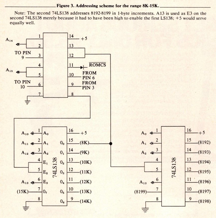
Figure 3 shows the LS00 and LS138 circuit to address the space from 8K to 15K. Reversing lines A15 and A13 in Figure 3 will address 32K to 39K.
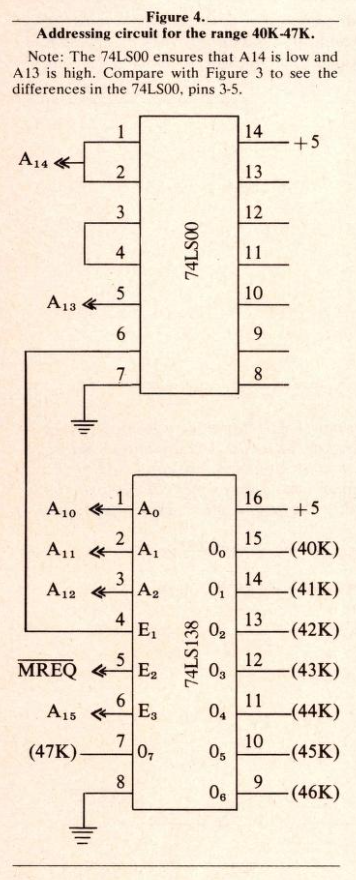
Figure 4 shows how to address 40K to 48K. The rest I will leave to the reader to design if he needs them. The idea is exactly the same.
The 74LS08 chip is used to combine two output lines from the LS138 in order to enable 2K devices such as a 2016 RAM chip, or multiple enable chips like the 8251 USART. Figure 3 shows how one 74LS138 is used to access the 8K to 16K space, and then a second is used to close the range to the byte level from 8192 to 8199. Addresses 8192 and 8193 can then be combined by a 74LS08 to activate an 8251 control or data port.
RAMCS and ROMCS
When you add memory chips from 16K upwards you will have to take the on-board RAM into consideration. If the RAM being added is in the form of 2K or 1K chips, it is obviously worth while to use the on-board RAM as well by connecting the first (16384) output pin of the LS138 (pin 15) to the Sinclair RAMCS line. If you have a TS1000 with 2K on board, you will have to connect the LS138 pins 15 and 14 to the inputs of an LS08, and the output from that circuit to RAMCS. Use the subsequent LS138 outputs to enable the new RAM chips. If you are adding 16K chips, the easiest solution is to connect RAMCS to +5 and forget the on-board RAM.
ROMCS is a somewhat different story. If the new chip addresses are from 16K to 32K, ignore this line entirely. The same goes for 48K to 64K. For the other addresses, the simplest method is to invert each chip select line from the LS138 which you intend to use (via a 74LS04), then connect the LSO4 output to a small diode (anode end) and connect the cathode to ROMCS. (The cathode end of a diode normally has a color band around it, usually black). If you omit the connection to ROMCS, the ROM will answer as well as your new chip, resulting in unexpected data being passed back to your program. If you omit the diode, the high value from the LS138 connected to the ROMCS when the LS138 is not being enabled going through the LS04 results in a permanent enable of the ROM, with strange results.
A Simple Tool
As a final note, it is possible to check out your address select circuits by building a very primitive logic probe with which to observe the state of the LS138 (or any other one-shot TTL) lines. Take the smallest LED you can find, and wire the long pin onto a handy +5 source and the short pin onto the select line you want to check. Power up the Sinclair and turn down the lights so you can see the LED flash, then type in PRINT PEEK xxxx where xxxx is the address that should select the line connected to the LED. If it flashes, you are OK. A short loop program that runs through the PEEK continuously will light the LED somewhat better. If the LED does not flash, hook it across +5 and ground to make sure it works, and check the wiring on the LS138 again. If it stays lit all the time, something is wrong with the enable wiring on the LS138 so it is enabled continuously.
Checking address and data lines this way is pointless since the keyboard scan routines in the ROM keep activating these lines constantly.
It is also possible to make up a circuit around a latching type chip (like a 4013) with a manual switch and connect that between the WAIT line and ground to ‘single-cycle’ the Sinclair. This will have the effect of ‘freezing’ each signal, but the thousands of machine cycles involved in a single PEEK would wear out your switch-pushing finger pretty quickly.
I hope that this discussion has helped to explain why the Sinclair reacts the way it does so that some of you will be able to add more good things to an already fine computer.


