The Unused 1K-2K Space
So, do those of you who have upgraded your ZX81/TS1000 to 16K ever feel sorry for that unused 1K-2K RAM, sitting unloved and unneeded inside your computer? Why not put it to work for you by wiring together this little circuit? It will convert your on-board RAM into a handy little place to put machine code programs, cost under $10, and, if you are handy, take about 15-30 minutes to wire up. Here, nestled away, will be a memory location unaffected by LOAD, NEW, and (with a little switch) MC induced crashes.
The on-board RAM begins at address 16384 (4000h) and it is deactivated when you plug in an external RAM pack. This is done by putting the +5 volts to the RAM chip select line (RAM CS), which turns off (deselects) the internal RAM chip. (The RAM chip is active or selected when RAM CS is low, i.e., close to 0 volts.) You can use this internal RAM at any address you desire, simply by making RAM CS low whenever a certain range of addresses is called for.
For machine code programmers a convenient place to use in the Sinclair memory map is the area 8192-16383, since it is not affected by LOADing or the NEW command. Ordinarily this area is occupied by the ROM operating system which selfishly repeats itself there out of its “normal’’ position between 0 and 8191. This was done apparently for simplicity of decoding—the Sinclair logic chip makes ROM CS low (i.e., turns on the ROM) whenever the A14 address line is low (therefore from addresses 0-16384 and again from 32768-49151).
Opening the 1K-2K Space
To free up some of this wasted space all you have to do is put ROM CS high whenever some of these addresses are needed, thus “turning off” the ROM in the same way a RAM pack turns off the internal RAM. With the ROM out of the way, we are then free to use this memory area.
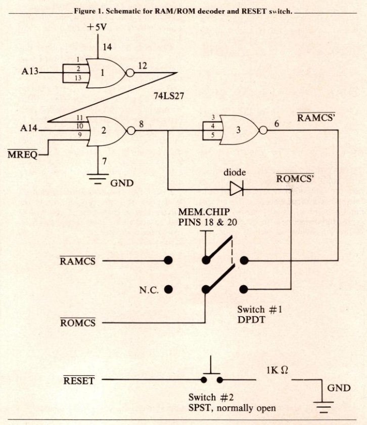
The circuit shown in Figure 1 utilizes this principle in a very simple fashion. (To learn a little about logic gates to follow this, see Radio Shack’s Engineers Notebook.) Using a single 3 input triple NOR gate chip (74LS27 or equivalent), you can easily decode and select/ deselect the RAM/ROM to utilize addresses 8192-16383.
The schematic shows that when A13 is high (i.e., equal to 213 or 8192) and when A14 is low (i.e., equal to 0) and when memory request (MREQ) is low, the output from the second NOR gate will be high. (MREQ goes low whenever the Z80 CPU “wants” to read from or write into memory.) !
Looking at it another way, the output from NOR gate #2 will be high whenever memory is requested from addresses 8192-16363 (or addresses 40960-49151, since the relationship A14 low, A13 high also occurs in that upper address area).
If we take this high output from NOR #2 (ROM CS) and put it to the ROM CS line on the board, the ROM will be turned off when the above memory locations are addressed. The diode shown in the schematic is necessary to prevent a low from enabling the ROM at inappropriate times, but it allows a high to get through when we want it.
We can take this same high output, put it through the third NOR gate (thus inverting it to a low—RAM CS’) and use it to enable our on-board RAM via the RAM CS pin (pin #18). You must first remove the RAM chip and bend out the RAM CS pin so that it no longer makes contact with the disabling +5 volts coming from your external RAM pack.
What you have after all this is your on-board RAM chip selected (i.e., ready to send or receive data) and your ROM deactivated whenever memory locations 8192-16383 or 40960-49151 are addressed. You have decoded a lot more memory area than you need for your 1K-2K RAM chip, but they are usually unused areas anyway.
Be aware, however, that some peripheral devices use the 8K-16K area in their hardware design, so in those cases this decoding scheme could give you some real problems. Consult your user’s manual if you have any extra hardware (other than a 16K RAM pack) before you jump into this modification. If it uses any memory locations in that area you had best leave this project alone.
Another theoretical note: you will note on the schematic that the signal to the RAM CS pin (pin 18 on a 1 or 2K chip) from the third NOR gate also goes to pin 20. This is the READ enable pin which can be held low, whether the RAM chip is being READ from or WRITTEN into. (There is also a WRITE enable pin on the memory chip which permits data to be written into RAM when low and read from RAM when it is high, as long as the READ enable pin is held low at all times.) Since the Timex/Sinclair circuit board ties together pins 18 and 20 (and thus to the RAM pack’s +5V), you have to disengage both of these pins from the socket and wire them together to your RAM CS’ signal.
The optional DPDT switch (switch #1) will allow you to switch back to the on-board RAM at its usual memory location when you are not using the 16K RAM pack. If you never want to use the on-board RAM without the RAM pack, then just wire the circuit in without the switch.
Adding a Reset Switch
If you have done much MC programming, you are probably painfully aware of how easily MC programs can crash your computer. Even if you have your MC program in the 8192-16383 area (where it is safe from NEW) and you crash the computer and unplug the power, good-by MC.
A simple way around this uses the RESET pin present on the Z80 CPU. This pin (pin #26) is held high at most times. If you temporarily pull this pin low, the CPU will stop what it was doing and will go back to the beginning of the ROM (address O), just as if you had just turned the power on.
During a crash, making RESET low will effectively get the computer going again, but, since the power was not interrupted, the MC program that you had in the 8192-16383 area will remain perfectly intact (and ready to crash your computer again!).
By connecting a momentary SPST switch (switch #2) and a 1K ohm resistor between RESET and ground, you will have a handy reset button to use in the event of a crash. Remember, however, that if you press reset at any other time you will wipe out your program above 16384, just as if you had pressed NEW.
Construction
Read these instructions all the way through before you actually begin so that you know what you are going to do.
1) Parts and tools.
You will need the following items:
- small Phillips head screwdriver
- A 15-25 watt fine tip soldering iron.
- Solder.
- 30 gauge wire-wrap wire and wire wrapping tool.
- 1 triple, 3 input NOR gate (74LS27). Available at most electronics supply houses, but not at Radio Shack.
- 14-pin DIP socket (solder tail type).
- 1 switching diode (1N914, R.S. 3: 276-1620 or other fast switching diode).
- DPDT switch (R.S. #275-403 or equiv.).
- SPST submini momentary, normally open switch (R.S. #2751571 or equiv.).
- 1 1000 ohm 1/4 watt resistor.
2) Wire the circuit.
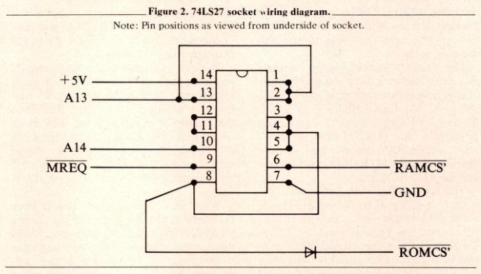
Following the circuit diagram (Figure 2), make the appropriate connections to the 74LS27. This is best accomplished by making them directly to the DIP socket. For connections that will be made to the Sinclair circuit board, solder 2-3 inch wire-wrap wire to the appropriate pins of the socket. Strip about 1/8” insulation from the ends of wires that will be soldered and about 3/4” from the wire that will go to the memory chip.
The diode can be soldered either to pin 8 of the socket or directly to the ROM CS hole on the board—your choice. Make sure you have it oriented in the right direction—usually the – banded end is the anode, i.e., the end that connects to the board.
Put the chip in the DIP socket, making certain that it is in right side up (i.e., Pin #1 in socket #1).
3) Remove the circuit board.
Remove the five phillips head screws from the base of the computer (three are under the lower and upper left rubber pads). Note that there are both long and short screws and make note of which ones go where. Remove the back and then the two screws holding the board in place. Carefully turn the board over and gently remove the keyboard tails. (Do not rip them!)
4) Locate landmarks.
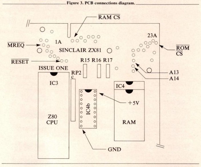
Match up the locations of the appropriate holes (PCB feed throughs) on the board as shown in Figure 3. Also look at the picture in your Sinclair Basic Programming book (same pictures in ZX81 and TS1000) and figure out which little black box is the RAM chip and which is the CPU.
If your computer is a ZX81, you may have two small RAM chips instead of one larger chip. You will still be able to do this project, but you will be a bit more cramped for space when it comes to placing the 74LS27.
Once you have located all the holes, make sure they are correct by checking continuity (preferably with a low-power ohm meter) between the holes and the appropriate pins of the CPU or ROM as follows:
Line         Chip       Pin
RESET        CPU         26
A14          CPU         4
A13          CPU         3
MREQ         CPU         19
RAM CS       RAM         18*
ROM CS       ROM         20
+5 volts     ROM         24
Ground       ROM         12
*or RAM pin 8 if two smaller RAM chips present.
5) Solder the appropriate wires to the board.
Use small amounts of solder to prevent solder shorts. Check both sides of board after each connection. Keep the leads of the diode short and insulate them with tape. Solder + 5V last.
It is a good idea to power up your computer after each connection and see if a K cursor still appears (you do not need the keyboard plugged in). If any shorts are present, you will get some squiggly lines or other such garbage on the screen. Desolder your most recent connection and try again if this happens.
6) Connect 74LS27 to RAM chip.
Remove the RAM chip from its socket by carefully prying up each end. (Do not bend the pins!) Once removed, bend out pins 18 and 20. (If you have 2 little RAM chips, remove them and bend out pin #8 only on each.)
Now wire-wrap the RAM CS’ wire from the 74LS27 to pins 18 and 20 (or pins #8—see above). Replace the RAM chip(s) in the socket(s) with the bent out pins sticking out sideways.
If you are using the DPDT switch shown in the schematic, make the connections as shown.
Before you actually wire it in, find a spot to mount your switch that will not get in the way of things when you are done. Since I have my computer in a large enclosure, I did not actually mount the switch on a “stock” chasis. The upper right corner of the front cover is probably a good location.
7) Reset button.
If you want to mount your SPST switch, find some out of the way place on the case, drill a hole, and mount it. Solder the 1K ohm resistor to one pole of the switch after trimming its leads as short as possible. (Insulating these leads with some electrician’s tape is probably a good idea to prevent shorts.) Connect the switch to the ground and RESET holes on the board, with the 1K ohm resistor wired in series as shown in the schematic.
8) Affix the 74LS27 assembly to the board. One easy way to do this is to tape it to the board, upside down, using double-sided tape or a small dab of rubber cement. This will keep the chip from bouncing around inside your computer, which would cause all kinds of mischief.
Testing
I would advise testing before you put your computer back together:
1) Reset button.
This is easy. A brief push of the button should give you a blank screen followed by the return of the “K” cursor. If a program was in memory, it will be gone.
2) New RAM area.
If the DPDT switch was used, switch 1t so that the RAM chip is connected to RAM CS”. Plug in your 16K RAM and enter this program to test it:
10 FOR N=8192 TO 10239*
20 POKE N,0
30 PRINT PEEK N;
40 NEXT N
* use 9215 if 1K RAM
This will POKE zeros into each memory location and verify it PRINT-PEEKing each byte. You should get about 2 1/2 screens full of zeros with a 2K RAM. (Since the entire 8K block from 8192 to 16383 is decoded, you will also get zeros if the space between 10239 and 16383 is PEEKed.)
If you are using a 32K RAM pack, you probably should POKE RAMTOP no higher than 40960 (the first 24K). Since our one-chip decoder repeats itself in half of the second 16K block (addresses 40960-49151), you may get into a data bus conflict if you try to use that area. Some RAM packs may work in this area however—try and see.
Now put the DPDT switch into the other position, remove your RAM pack, and turn on the computer. It should now work just like it used to without the RAM pack.
Trouble shooting
Recheck your connections! There is really little else that can go wrong other than wrong/bad connections and solder shorts. Did you make all of the right connections to the board? Is the chip or diode in backwards? If the computer will not work at all, then unsolder your connections one by one, testing the computer after each step. Write me if even the above does not help.
If you succeeded with this little project, you now have a sequestered place to put the machine code, and also a way to keep it there after it crashes your computer. You will also have learned a little bit (byte?) about the ZX/TS circuitry and have experienced some of the more intangible rewards of becoming a “computer hardware hack.”


