
Simulation Circuits and Timing Charts of the SCL Chip
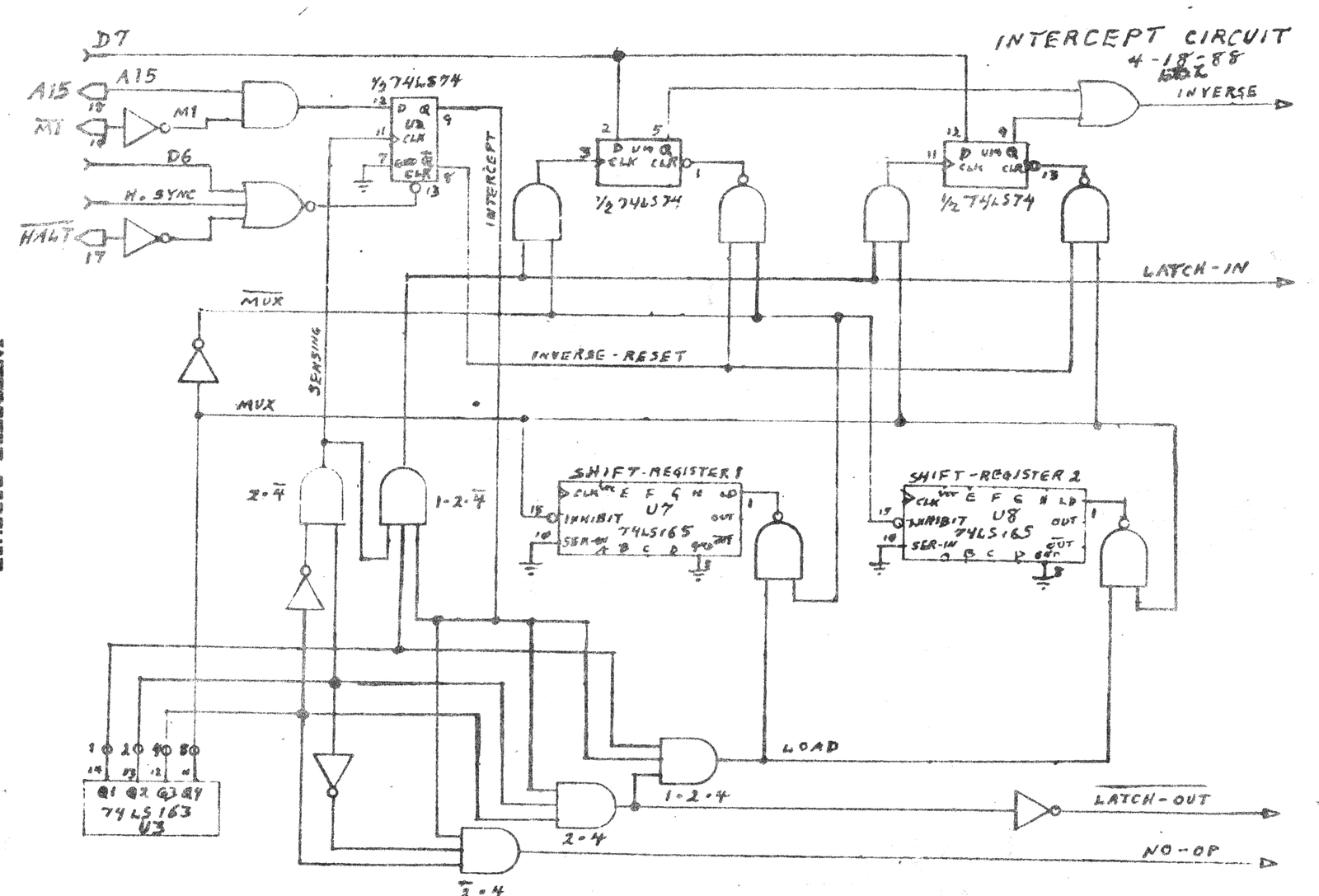
Being unable to draw the exact circuits; because of the lack of any technical data on the Ferranti Mask Programmable Universal Logic Chip ULA2C184E (either programmed or unprogrammed); using standard TTL chips I have made the following drawings simulating the functions that the ROM routines indicate.
         ULA2C184E  Pin-out Chart
                   1C-1
                 SCL CHIP

 1    A7' --->            40    +5V
 2    A8' --->            39    A6' --->
 3    A2' --->            38    A5' --->
 4    A1' --->            37    A4' --->
 5    A0' --->            36    A3' --->
 6    RD <---             35    CLOCK
 7    IORQ <---           34    GND
 8    WR <---             33    KBD0 <---
 9    MREQ <---           32    D0 <--->
10    M1 <---             31    KBD1 <---
11    A14 <---            30    D1 <--->
12    RAMC.S. --->        29    KBD2 <---
13    ROMC.S. --->        28    D2 <--->
14    CLOCK' --->         27    KBD3 <---
15    NMI --->            26    D3 <--->
16    TV/TAPE --->        25    KBD4 <---
17    HALT <---           24    D4 <--->
18    A15 <---            23    D5 <--->
19    D7 <--->            22    USA/UK <---GRD FOR USA
20    TAPE IN <---        21    D6 <--->

fclock = 6.5 MHz
fclock' = 3.25 MHz
Editor’s note: Due the amount of drawings, several will be included in the Mar/Apr 89 issue of SINCUS NEWS, with the rest of Don’s notes. In the above artwork- there are lines over RD, WR, MREQ, RAMC.S., ROMC.S., HALT NMI, and M1.
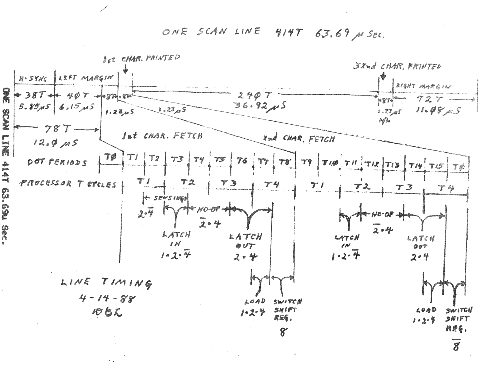
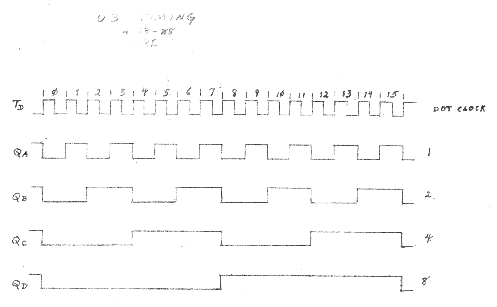
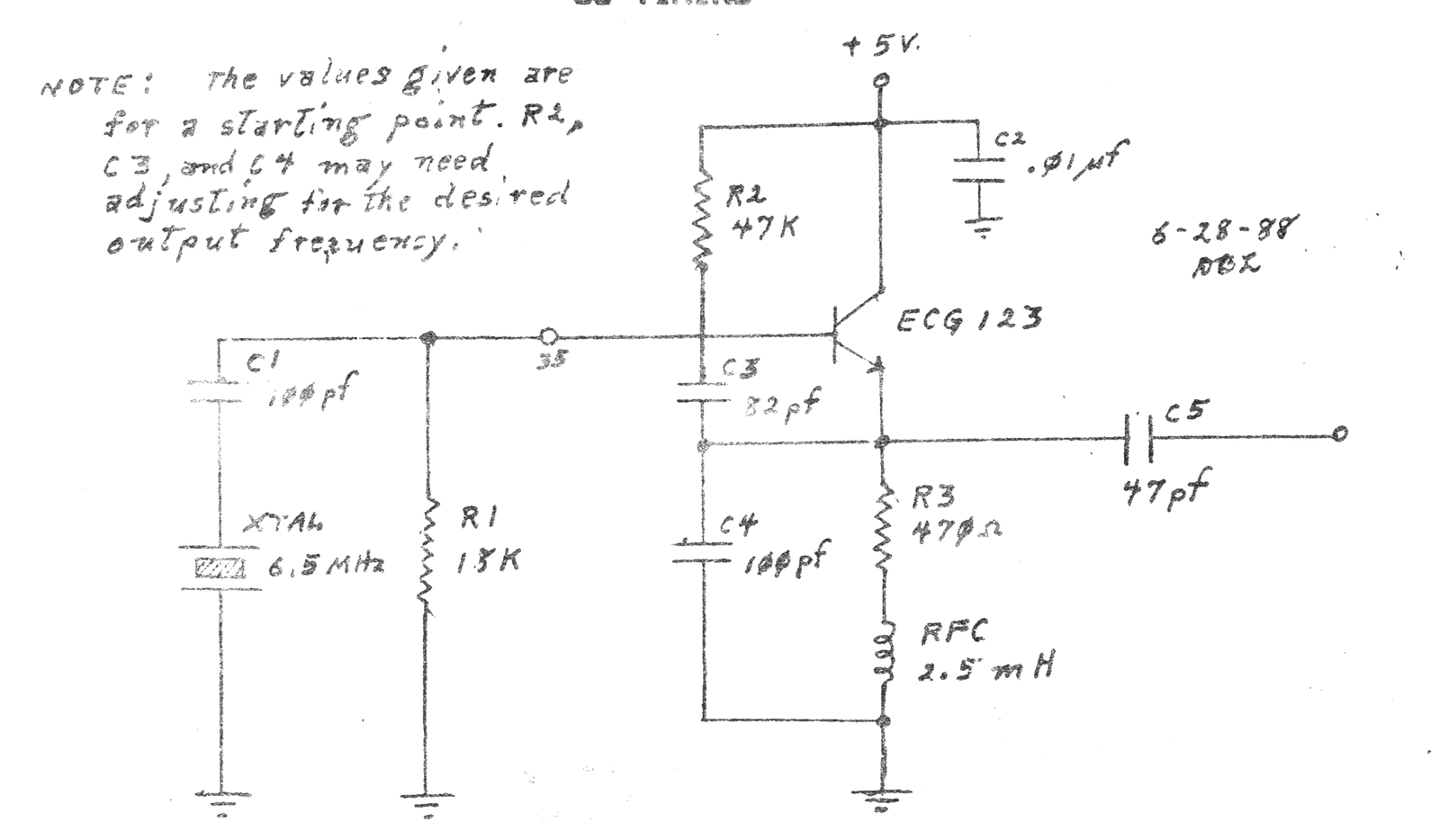
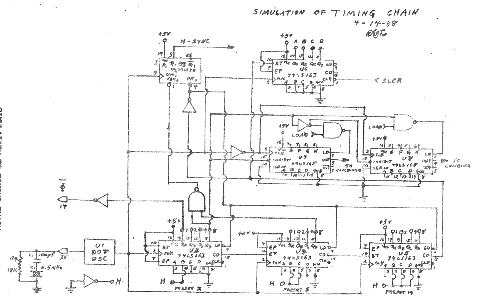
PARAMETERS
Dot Clock Frequency:  6.5 MHz  + or -  200 Hz
Processor Clock Frequency:  3.25 MHz  + or -  100 Hz
Dot Period (Td):  0.1538451 uSec.  + or -  4.7 pSec.
Processor Clock Period (Tp):  0.3076923 uSec. + or - 9.4 pSec.
Horizontal Sync Pulse:  19 Tp = 5.85 uSec.
Horizontal Scan Line:  207 Tp = 63.69 uSec.
Frame Sync Pulse:  1212 Tp = 372.92 uSec.
One Frame:  54234 Tp = 16687.384 uSec.
          1/60 Sec. = 16666.6 uSec.
    Therefore: The Frame Time is 0.12 %  Slow, well within  the allowable 2 %.
    Normal Horizontal TV Scan = 63.4 uSec.
    Therefore: The Horizontal Scan Time of the T/S 1000 (63.69 uSec.) is 0.46 %
  Slow, also well within the allowable 2 % .
NOTE: After the first Frame, each Frame equals exactly 262 ScanLines.
INTERRUPT TIMING
NMI:
1. If NOT NMI is Low and NOT HALT is Low the Instruction Execution Time 11 Tp (The same as a normal RST instruction).
2. If NOT NMI is Low and NOT HALT is High the Wait circuit built around transister TR-1 pulls the NOT WAIT Pin of the Z-80 Low. The M1 cycle of the NMI instruction does not poll the NOT WAIT Pin. Therefore the NOT WAIT signal is not detected until T2 of M2, a WRITE cycle, which is the 7th T cycle of the instruction. This leaves 5 T cycles to be completed after the NOT NMI Pin goes High. Therefore, the execution time of this instruction is equal to the Horizontal Sync + 5 Tp (24 Tp).
INT:
1. In Interrupt Mode 0 the execution time is 2 Tp more than the normal execution time for the instruction being entered by the peripheral. This is because there are two built in wait states in this interrupt.
2. In Interrupt Mode 1 the execution time is 13 Tp, two more than a normal RST instruction because of the two built in wait states.
3. In Interrupt Mode 2 the execution time is 19 Tp. 4. The Maskable Interrupt polls the NOT WAIT line on the 2nd built in WAIT T cyle of M1. If the NOT WAIT line is pulled Low late it can also be detected during T2 of either M2 or M3.
NOTE:
1. Both NMI and INT have a T1, T2, T3, T4 & T5 in M1 and T1, T2 & T3 in both M2 & M3.
2. In INT the built in wait states are between T2 & T3 of M1.
Part 3 will conclude this series on the TS1000 SCL Chip in the Mar/Apr 89 issue.