Mr. Frank Davis
Editor UPDATE!
513 E. Main St.
Peru, IN 46970
9/24/92
Dear Frank,
The latches must be already reset and ready before the CPU comes on line. CMOS chips usually automatically reset on power-up, so it wasn’t certain that applying the RESET signal was even necessary.
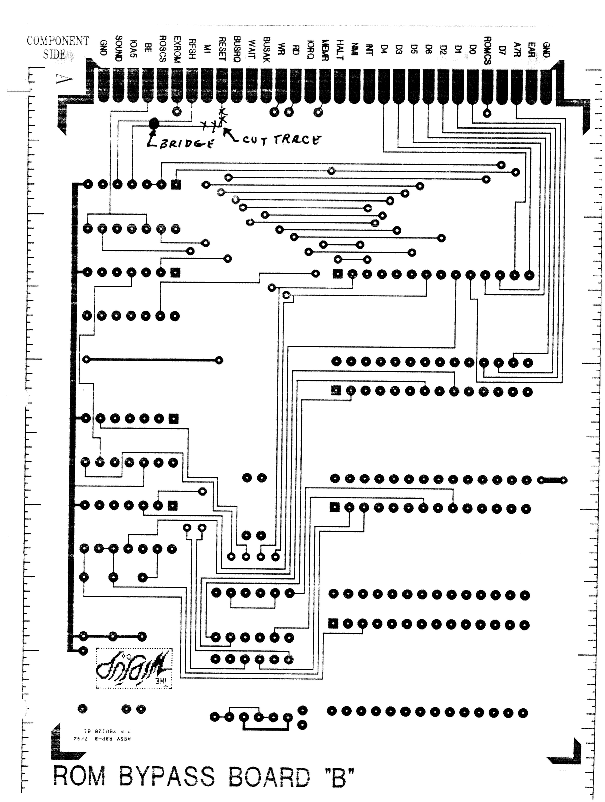
The thing to try was to cut the RESET trace and jumper pins 3 and 4 on U4. If no problem, leave it that way.
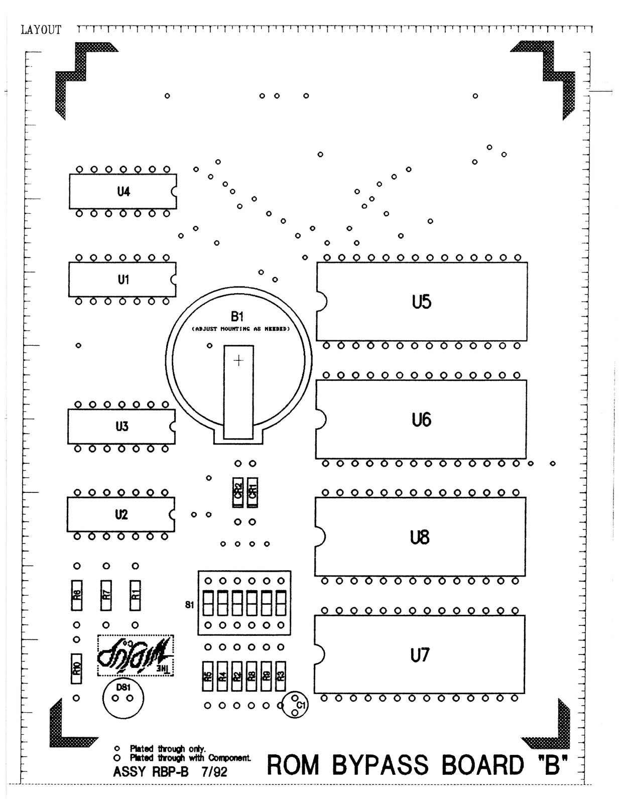
Well, there was no problem, so that’s it. See the marked PCB trace for all that’s needed. For such a complex board, I think it came up smelling like a rose (barring Murphy).
The 138 (and relocated U4) can be added later on a piggy-back daughter board (using a wire wrap socket). For now, the ROMCS trace will not be cut, nor will ROSCS be brought from the edge using a wire.
Boards can be updated later if desired.
Larry Crawford has verified total success using plugged in EPROMS. He has not yet verified using SRAM as ROM. Even the HOT-Z cartridge works with either DOS in place.
The acid test has been passed, yet much needs to be done. Most important is to get far enough along with new ROMs so results can be demonstrated before hackers get an opportunity to misuse their new toy.
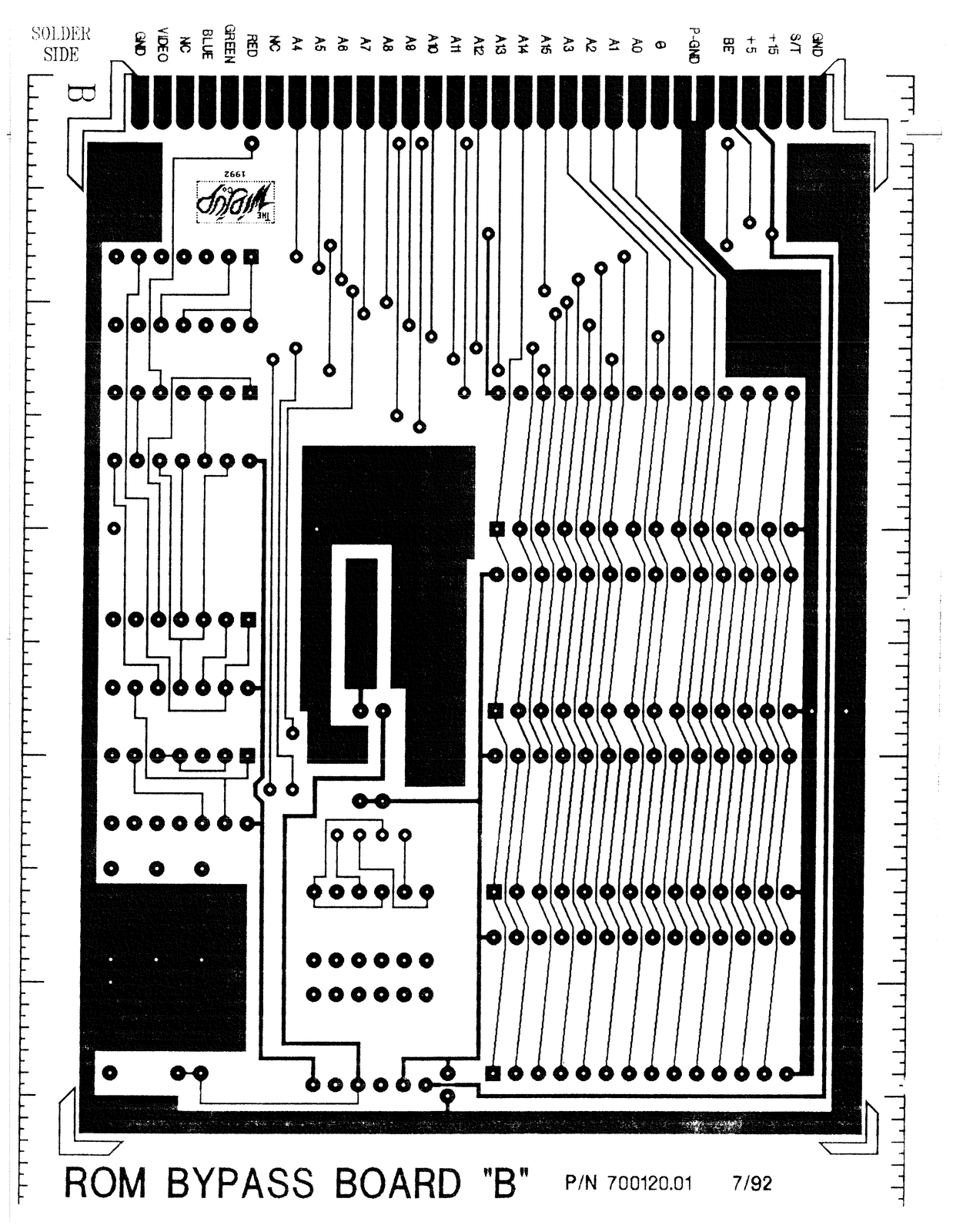
Still, it is imperative to announce the sucess of this project, and to show the schematic for the version that requires getting inside the TS2068 to rewire it. That won’t give away the details on how to get it to work without touching a screw and should discourage those who might be tempted by avarice. You could even publish the board patterns after using white-out on those alterations.
An editorial comment would carry a lot more weight than what I could say, and technical explanations are inapropos at this time.
Rumors are spreading anyway, so it is better to confirm them in a manner that will inspire serious interest in the TS2068, not as just another gadget to play with.
A problem with my plugging it is: “I TOLD you so!”. To say that in print would feel so good.
Larry has promised to alter the board you send me for the no-screw-touched version but for him to do that he needs both boards, as he only has Oliger style buss extenders. Only then will I be able to begin work on ROM repairs in earnest.