Authors
Publication
Pub Details
Date
Pages
Enclosed are copies of “ctas.Bl” v9.2. If you have sent copies of the previous version to anyone and happen to have a record of who, send me his name and address and I’ll mail him the latest version.
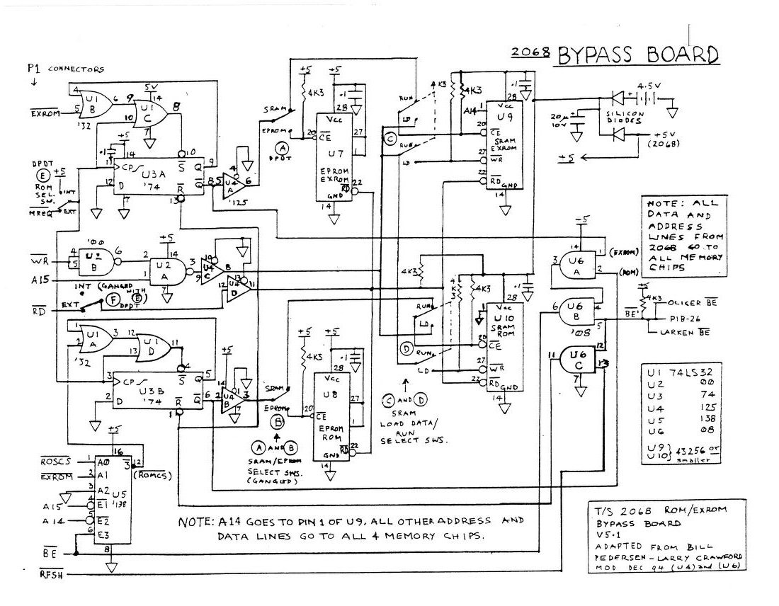
Also enclosed is a schematic of ray working version of Bill’s ROM/EXROM bypass board. In case you ever have time to look at it, I’ll lead you through its operation in the Tas file “bypass . CT”.
Note that the E3 enable pin of the LS138 is connected to the BE line, not +5v. I told Bill that his version did not work in real life, but I guess that he had already printed his latest schematic or still believed in his logic. I replaced his DIP switches with DPDT toggles which are so much more convenient to use (especially since my board is installed in behind other boards and the DIP switches would be physically inaccessible).
The toggles also look after the “deaf” and “dumb” states of the various control pins of the memories automatically, eliminating the possible confusion inherent in setting each one manually.
It took me many hours to prove out the many possible variations of it since my board is hand-wired and every time I made a mod, I managed to create a solder bridge or melted the insulation on a couple of overlapping wires so that they shorted or one of the wires came unsoldered. It was a very frustrating experience but the circuit conforms to Bill’s logic and works fine at last.
I said in my last note that the RFSH signal was not needed. All my programs ran fine without it, but Bill must have had a good reason to include it, so I put it back in.
ROM AND EXROM BYPASS BOARD INFORMATION
Way back in 1988, Bill Pedersen reasoned correctly that it should be possible to disable the HOME ROM and EXROM and enable other ROMs external to the 2068. This process could be done without opening the computer case.
HOME ROM can be disabled by driving the BE line low. This is accomplished by the 74LS08 AND gate U6B. Its output at pin 6 will be low if the output of either the LARKEN or Oliger DOS board is low (and other conditions which will be covered later). To implement this, since there is not an unused edge connector in the slot, the the LARKEN board must be patched onto a board which can be plugged into an expansion slot at the rear of the 2068. The BE line must be cut between the large diode and the edge connector and the diode connected to the center pole of a SPDT switch. The output (anode end of the diode) can then be switched to PlA-29 for normal internal operation with the bypass board removed or to PlB-26, an unused PI connector. This line is designated BE’ NOT and will take over control of the computer at power-up if the bypass board is installed.
Since the Oliger board is already on an expansion slot board, it needs only to have its BE output switched to the same PI connectors .
When the system is booted, the DOS boards, which are located in the DOCK bank, have priority and drive the BE line low (U6B-pin 6) and reset the 74LS74 flip-flops (U6C-pin 11). At this time the Q outputs are low and the Q NOTs high thus making the BE line high so that the SCLD can send out an EXROM enable signal. The flip-flops are also reset by U6C during a REFRESH cycle.
HOW THE EXTERNAL EXROM GETS CONTROLLED
When the EXROM line goes low, the MREQ line will already be low. Thus the 74LS32 gates U1B & U1C SET flip-flop A, making the Q output high. This effectively latches the flip-flop outputs. Since Q NOT is low, the external EXROM is enabled and the BE line driven low by gates U6A & U6B, disabling both HOME EXROM and the 74LS138 decoder. Thus the external EXROM stays active until the MREQ line goes high. At this time the CP input makes a low-to-high transition and resets the flip-flop. Since the DATA input is grounded, Q goes low and Q not goes high. This disables the external EXROM and makes the BE line high, allowing the SCLD to operate normally.
HOME ROM
The HOME ROM is controlled by the ROSCS signal from the SCLD. Unfortunately, this line is not available at the PI connector. However, it can be simulated by the use of a 74LS138 decoder. It has three enable inputs and three data inputs. The decoded output is driven low. All others are high.
HOME ROM will be active when BE NOT is high, A14 and A15 are low, and ROSCS NOT, EXROM NOT, and RFSH are high. Under these conditions, CHUNKS 0 and 1 are being addressed and both the DOCK and EXROM banks are inactive.
HOW EXTERNAL ROM GETS CONTROLLED
Since ENABLE E3 of the 74LS138 decoder is high, if A14 and A15 are both low, the ‘138 will be enabled. Then if the ROSCS and EXROM lines are both high, output 3 will go low, simulating an active ROMCS line. This is applied to one of the inputs of OR gate UlA. The rest of the sequence of events is the same as for control of the the external EXROM.
OTHER LOGIC COMPONENTS
Functions of the bypass board are controlled by by four DPDT toggle switches:
E&F select internal or external operation. When the board is first tried out, set them for internal operation. Switch E disconnects the MREQ line from the flip-flops and connects the CP inputs of the flip-flops to the 5v buss. This keeps them from being reset by a ROM or EXROM request. At the same time, switch F disconnects the RD line from all four memory chips on the board. This prevents spurious data from being read and confusing the system. The computer should operate as if the board were not installed.
A&B set the board for either EPROM or SRAM operation. The buffered Q NOT outputs of the flip-flops are routed to the CE pins of the appropriate memory chips.
C&D select operation so as to run the code in the SRAMS or to load code into either one.
THE 74LS125 TRI-STATE BUFFERS
This chip was added to keep the backup battery drain to about 2 microamps when the computer is turned off. Otherwise, about 2 ma leak back through the other ICs, shortening the battery life significantly.
LOADING CODE INTO THE SRAMS
- Select SRAM operation. ( SWs A/B)
- Select INTERNAL operation. (SWs E/F)
- Select ROM to LOAD. { SW D )
- Load ROM code to 32768.
- Switch D to RUN.
- Select EXROM to LOAD. (SW C)
- LOad EXROM code to 32768.
- Switch C to RUN.
- Select EXTERNAL operation. (SWs E/F)
- Reboot the computer.
Loading of the codes is probably best done with a simple Loader Program stored on the same disk as the ROM and EXROM codes. Here is an example:
   10 REM EXTERNAL ROM AND EXROM LOADER
   20 CLS: PRINT AT 10,5; "LOAD ROM OR EXROM? (R or X)": POKE 23658,0: INPUT a$
   30 IF a$="r" THEN RANDOMIZE USR 100: LOAD "ROM. C1" CODE 32768: STOP
   40 IF a$="x" THEN RANDOMIZE USR 100: LOAD "XROM.C1" CODE 32768
 9998 STOP
 9999 RANDOMIZE USR 100: SAVE "ex-r/x.Bl" LINE 1
If both SRAMS are to be loaded, RUN the program and select the ROM switch to LOAD before responding “r” to the prompt. Switch to RUN. RUN the program again and select the EXROM switch to LOAD before responding “x”. Switch to RUN and select EXTERNAL operation .
Note that the ROM is controlled by the SCLD which can address only 16K. Thus this is the maximum size of the external ROM.
Since the external EXROM is fully addressed, the maximum size of it is 32K.
Note that even though the codes are loaded to 32768, both the ROMs will run as shadows of the internal ones. Thus the external ROM will be called at 0000 by the SCLD at power-up.
WHY THE EPROMS?
Using the SRAMS is a very convenient way of making and testing changes to the ROMs. After the changes have been proven, EPROMS can be made and installed on the board. The backup battery can then be removed and switches A&B left in the EPROM position,
BOOTING THE SYSTEM WHEN THE EXTERNAL BOARD IS SELECTED
On power-up, the SCLD could be calling the EXROM, In which case, the 2068 will not be comletely initialized. A proper solution would be to modify the EXROM codes so as to send control back to address 0000 of the ROM. For now, turn on the disk drives before the computer. If the ready light for drive 0 does not come on, reboot the computer. It may take 2 or 3 attempts to get it all together.